always @(posedge clk_Modulation) begin if (reset == 1'b1) begin tx_conv_encoder_valid_dly <= 1'b0; tx_conv_encoder_bit_dly <= 1'b0; end elsebegin tx_conv_encoder_valid_dly <= tx_conv_encoder_valid; tx_conv_encoder_bit_dly <= tx_conv_encoder_bit; end end
//----------------conv_sft------------------ always @(posedge clk_Modulation) begin if (reset == 1'b1) begin conv_sft <= 'd0; end elseif(tx_conv_valid_neg_pls)begin conv_sft <= 'd0; end elseif(tx_conv_encoder_valid)begin conv_sft <= {conv_sft[5:0], tx_conv_encoder_bit}; end end
//----------------tx_conv_valid_dly------------------ always @(posedge clk_Modulation) begin tx_conv_valid_dly <= tx_conv_valid; end assign tx_conv_valid_neg_pls = tx_conv_valid_dly & (~tx_conv_valid);
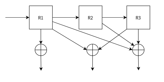
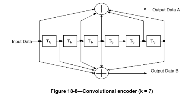
//-------------tx_conv_bit_a/b--------------------- always @(posedge clk_Modulation) begin if (reset == 1'b1) begin tx_conv_bit_a <= 1'b0; tx_conv_bit_b <= 1'b0; end elseif(tx_conv_valid_neg_pls)begin tx_conv_bit_a <= 1'b0; tx_conv_bit_b <= 1'b0; end elseif(tx_conv_encoder_valid_dly)begin tx_conv_bit_a <= (conv_sft[6]&conv_coef1[6]) ^(conv_sft[5]&conv_coef1[5]) ^ (conv_sft[4]&conv_coef1[4])^ (conv_sft[3]&conv_coef1[3]) ^(conv_sft[2]&conv_coef1[2]) ^(conv_sft[1]&conv_coef1[1]) ^ (conv_sft[0]&conv_coef1[0]) ; tx_conv_bit_b <= (conv_sft[6]&conv_coef2[6]) ^(conv_sft[5]&conv_coef2[5]) ^ (conv_sft[4]&conv_coef2[4])^ (conv_sft[3]&conv_coef2[3]) ^(conv_sft[2]&conv_coef2[2]) ^(conv_sft[1]&conv_coef2[1]) ^ (conv_sft[0]&conv_coef2[0]) ; end end
//----------------tx_conv_valid------------------ always @(posedge clk_Modulation) begin if(reset == 1'b1)begin tx_conv_valid <= 1'b0; end elsebegin tx_conv_valid <= tx_conv_encoder_valid_dly; end end
fifo_generator_tx_puncture u_fifo_generator_tx_puncture ( .clk(clk_Modulation), // input wire clk .srst(reset), // input wire srst .din(tx_conv_bit), // input wire [1 : 0] din .wr_en(tx_conv_valid), // input wire wr_en .rd_en(fifo_rd_en), // input wire rd_en .dout(fifo_dout), // output wire [1 : 0] dout .full(full), // output wire full .empty(empty) // output wire empty ); //----------------puncture_flag------------------ always @(posedge clk_Modulation) begin if (reset == 1'b1) begin puncture_flag <= 1'b0; end elseif(empty == 1'b0)begin puncture_flag <= 1'b1; end elsebegin puncture_flag <= 1'b0; end end
//----------------cnt_puncture------------------ // the ofdm symbole is 216bit, so there is no doubt that // when the valid bit is finished, the counter will go back to zero: 0000000123,0123....0123000000 always @(posedge clk_Modulation) begin if (reset == 1'b1) begin cnt_puncture <= 'd0; end elseif(puncture_flag == 1'b1)begin if(cnt_puncture == 'd3)begin cnt_puncture <= 'd0; end elsebegin cnt_puncture <= cnt_puncture + 1'b1; end end elsebegin cnt_puncture <= 'd0; end end
always @(*) begin if(empty==1'b0 && puncture_flag == 1'b1)begin case(cnt_puncture) 0: fifo_rd_en = 1'b1; 1: fifo_rd_en = 1'b0; 2: fifo_rd_en = 1'b1; 3: fifo_rd_en = 1'b1; default : fifo_rd_en = 1'b0; endcase end elsebegin fifo_rd_en = 1'b0; end end
always @(posedge clk_Modulation) begin fifo_dout_dly <= fifo_dout; end
always @(posedge clk_Modulation) begin if (reset == 1'b1) begin tx_puncture_bit <= 1'b0; end elseif(empty==1'b0 && puncture_flag == 1'b1)begin case(cnt_puncture) 0: tx_puncture_bit <= fifo_dout[1]; 1: tx_puncture_bit <= fifo_dout_dly[0]; 2: tx_puncture_bit <= fifo_dout[1]; 3: tx_puncture_bit <= fifo_dout[0]; default: tx_puncture_bit <= 1'b0; endcase end elsebegin tx_puncture_bit <= 1'b0; end end
always @(posedge clk_Modulation) begin if (reset == 1'b1) begin tx_puncture_valid <= 1'b0; end elseif(empty==1'b0 && puncture_flag == 1'b1)begin tx_puncture_valid <= 1'b1; end elsebegin tx_puncture_valid <= 1'b0; end end
always @(posedge clk_Modulation) begin tx_puncture_valid_dly <= tx_puncture_valid; end assign tx_puncture_valid_neg_pls = (tx_puncture_valid_dly)&(~tx_puncture_valid);
always @(posedge clk_Modulation) begin if(reset == 1'b1)begin cnt_bit <= 'd0; end elseif(tx_puncture_valid == 1'b1)begin cnt_bit <= cnt_bit + 1'b1; end elsebegin cnt_bit <= 'd0; end end